 MENU
MENU 

Nextgen computing: Hard-to-move quasiparticles glide up pyramid edges
A new kind of “wire” for moving excitons, developed at the University of Michigan, could help enable a new class of devices, perhaps including room temperature quantum computers.
What’s more, the team observed a dramatic violation of Einstein’s relation, used to describe how particles spread out in space, and leveraged it to move excitons in much smaller packages than previously possible.
“Nature uses excitons in photosynthesis. We use excitons in OLED displays and some LEDs and solar cells,” said Parag Deotare, co-corresponding author of the study in ACS Nano supervising the experimental work, and an Associate Professor of Electrical and Computer Engineering. “The ability to move excitons where we want will help us improve the efficiency of devices that already use excitons and expand excitonics into computing.”
The ability to move excitons where we want will help us improve the efficiency of devices that already use excitons and expand excitonics into computing.
Prof. Parag Deotare
An exciton can be thought of as a particle (hence quasiparticle), but it’s really an electron linked with a positively-charged empty space in the lattice of the material (a “hole”). Because an exciton has no net electrical charge, moving excitons are not affected by parasitic capacitances, an electrical interaction between neighboring components in a device that causes energy losses. Excitons are also easy to convert to and from light, so they open the way for extremely fast and efficient computers that use a combination of optics and excitonics, rather than electronics.
This combination could help enable room temperature quantum computing, said Mackillo Kira, co-corresponding author of the study supervising the theory, and a Professor of Electrical and Computer Engineering. Excitons can encode quantum information, and they can hang onto it longer than electrons can inside a semiconductor. But that time is still measured in picoseconds (10-12 seconds) at best, so Kira and others are figuring out how to use femtosecond laser pulses (10-15 seconds) to process information.
“Full quantum-information applications remain challenging because degradation of quantum information is too fast for ordinary electronics,” he said. “We are currently exploring lightwave electronics as a means to supercharge excitonics with extremely fast processing capabilities.”
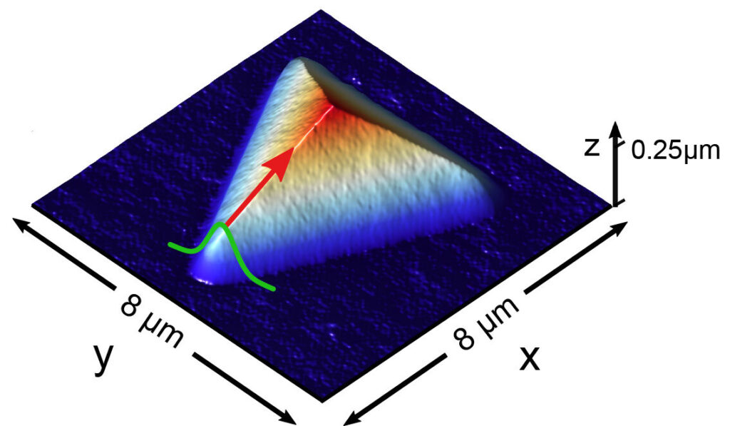
However, the lack of net charge also makes excitons very difficult to move. Previously, Deotare had led a study that pushed excitons through semiconductors with acoustic waves. Now, a pyramid structure enables more precise transport for smaller numbers of excitons, confined to one dimension like a wire.
It works like this:
The team used a laser to create a cloud of excitons at a corner of the pyramid’s base, bouncing electrons out of the valence band of a semiconductor into the conduction band—but the negatively charged electrons are still attracted to the positively charged holes left behind in the valence band. The semiconductor is a single layer of tungsten diselenide semiconductor, just three atoms thick, draped over the pyramid like a stretchy cloth. And the stretch in the semiconductor changes the energy landscape that the excitons experience.
It seems counterintuitive that the excitons should ride up the pyramid’s edge and settle at the peak when we imagine an energy landscape chiefly governed by gravity. But instead, the landscape is governed by how far apart the valence and conduction bands of the semiconductor are. The energy gap between the two, also known as the semiconductor’s band gap, shrinks where the semiconductor is stretched. The excitons migrate to the lowest energy state, funneled onto the pyramid’s edge where they then rise to its peak.
Usually, an equation penned by Einstein is good at describing how a bunch of particles diffuses outward and drifts. However, the semiconductor was imperfect, and those defects acted as traps that would nab some of the excitons as they tried to drift by. Because the defects at the trailing side of the exciton cloud were filled in, that side of the distribution diffused outward as predicted. The leading edge, however, did not extend so far. Einstein’s relation was off by more than a factor of 10.
“We’re not saying Einstein was wrong, but we have shown that in complicated cases like this, we shouldn’t be using his relation to predict the mobility of excitons from the diffusion,” said Matthias Florian, co-first-author of the study and a Research Investigator in Electrical and Computer Engineering, working under Kira.
We’re not saying Einstein was wrong, but we have shown that in complicated cases like this, we shouldn’t be using his relation to predict the mobility of excitons from the diffusion.
Matthias Florian, ECE Research Investigator
To directly measure both, the team needed to detect single photons, emitted when the bound electrons and holes spontaneously recombined. Using time-of-flight measurements, they also figured out where the photons came from precisely enough to measure the distribution of excitons within the cloud.
The study, “Enhanced exciton-drift transport through suppressed diffusion in one-dimensional guides,” was supported by the Army Research Office (award no. W911NF2110207) and the Air Force Office of Scientific Research (award no. FA995-22-1-0530).
The pyramid structure was built in the Lurie Nanofabrication Facility.
The team has applied for patent protection with the assistance of U-M Innovation Partnerships and is seeking partners to bring the technology to market.